Printed Circuit Boards (PCBs) are the backbone of nearly every modern electronic device. From smartphones and medical equipment to industrial automation systems and consumer electronics, PCBs provide the structural and electrical foundation that allows components to communicate and function efficiently. As electronic devices continue to shrink, increase in speed, and become more complex, PCB production methods have also advanced significantly.
Modern PCB manufacturing techniques combine precision engineering, advanced materials, and automated processes to produce reliable circuit boards capable of supporting high-performance electronics. Engineers working in electronics design or manufacturing must understand how these techniques influence performance, durability, and scalability in electronic products.
This article explores the most important modern PCB manufacturing techniques every engineer should know, including fabrication processes, advanced technologies like HDI boards, automated assembly methods, and the importance of quality assurance throughout the PCB fabrication process.
Understanding the PCB Manufacturing Process
Before exploring advanced technologies, it is important to understand the fundamental PCB manufacturing process. PCB fabrication involves multiple carefully controlled steps that transform a digital circuit design into a physical board capable of supporting electronic components.
The process typically begins with circuit design files generated using PCB design software. These files define copper traces, component placement, and layer configurations. Once finalized, the design moves to the manufacturing stage, where copper-clad laminate materials are prepared.
Next comes the photolithography stage. In this process, a photosensitive film is applied to the board and exposed to ultraviolet light through a mask that represents the circuit pattern. This exposure allows manufacturers to define copper traces precisely on the board surface.
The board then undergoes PCB etching, which removes unwanted copper while leaving the intended conductive pathways intact. After etching, drilling machines create holes for vias and component leads. Multilayer boards require lamination processes that bond several layers together under heat and pressure.
Finally, solder masks and silkscreen markings are added to protect the circuitry and identify components. These stages collectively form the foundation of modern PCB production technology.
Key Modern PCB Manufacturing Techniques
Advances in electronics have pushed manufacturers to develop new techniques capable of supporting smaller components, higher frequencies, and more complex circuit layouts. Several modern methods now play a critical role in the industry.
High-Density Interconnect (HDI) Technology
High-Density Interconnect technology is one of the most significant innovations in advanced PCB manufacturing methods. HDI boards allow designers to create compact circuits with extremely high component density while maintaining excellent electrical performance.
HDI boards use microvias, blind vias, and buried vias to connect different circuit layers. Microvias are extremely small holes created using laser drilling technology. Because they take up less space than traditional through-hole vias, engineers can route more signals through a smaller board area.
This manufacturing technique is widely used in smartphones, wearable devices, and high-speed computing systems. HDI technology enables improved signal integrity, reduced electromagnetic interference, and more efficient routing of complex circuits.
Surface Mount Technology (SMT)
Surface Mount Technology, commonly known as SMT, has transformed PCB assembly over the past few decades. Instead of inserting component leads through holes in the board, SMT components are mounted directly onto the surface of the PCB.
Automated machines place components onto solder paste applied to copper pads. The board then passes through a reflow oven where the solder melts and permanently secures the components.
SMT offers several advantages compared to traditional through-hole technology. It allows for smaller components, higher component density, and faster automated assembly. Most modern electronics rely heavily on SMT due to its efficiency and compatibility with automated production lines.
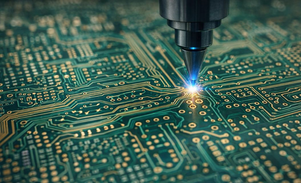
Laser Drilling for Microvias
Laser drilling has become an essential part of modern PCB manufacturing techniques, particularly for HDI boards. Traditional mechanical drilling methods cannot create extremely small holes required for microvias.
Laser drilling machines use high-energy beams to create precise holes with diameters as small as 75 microns. These microvias allow electrical connections between layers without occupying excessive board space.
Laser drilling improves routing flexibility, reduces signal path lengths, and enables the compact designs demanded by modern electronics. Many advanced electronics manufacturers now rely on laser drilling as a standard step in the PCB fabrication process.
Advanced PCB Lamination Techniques
Multilayer PCBs require lamination processes that bond several copper and insulating layers together. Advanced lamination techniques use controlled temperature and pressure to ensure proper bonding while maintaining precise alignment between layers.
Sequential lamination is commonly used in HDI boards. This process builds the PCB layer by layer rather than laminating all layers simultaneously. Sequential lamination allows manufacturers to integrate microvias and complex routing structures more effectively.
Modern lamination systems use automated alignment and vacuum technologies to prevent air bubbles or misalignment, ensuring consistent board quality.
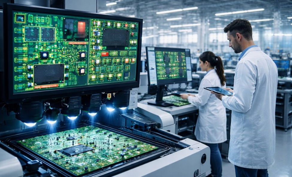
Automated Optical Inspection (AOI)
Quality control plays a critical role in PCB manufacturing, especially as circuit complexity increases. Automated Optical Inspection systems help manufacturers detect defects early in the production process.
AOI machines use high-resolution cameras and advanced image processing software to inspect boards for issues such as missing components, incorrect placements, solder defects, or damaged traces.
By identifying problems before final assembly, AOI improves production efficiency and reduces the risk of defective products reaching the market.
Materials Used in Modern PCB Manufacturing
Material selection plays a major role in determining PCB performance and reliability. The most common base material used in PCB fabrication is FR-4, a fiberglass-reinforced epoxy laminate that offers good electrical insulation and mechanical strength.
Copper foil forms the conductive pathways on the board and is available in different thicknesses depending on current requirements. High-frequency applications sometimes require specialized materials such as PTFE or ceramic substrates to maintain signal integrity.
Solder masks protect copper traces from oxidation and prevent solder bridges during assembly. Silkscreen layers provide component labels and manufacturing information.
Advanced PCB production technology often incorporates materials designed for thermal management, high-frequency performance, or flexible applications.
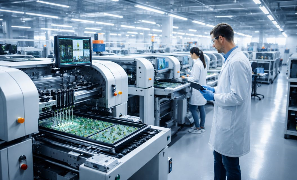
Automated PCB Assembly and Manufacturing Efficiency
Automation has become a defining feature of modern PCB production technology. Automated assembly lines use pick-and-place machines capable of positioning thousands of components per hour with extremely high accuracy.
These machines rely on computer vision systems to align components precisely with PCB pads. Once components are placed, reflow soldering permanently bonds them to the board.
Automation improves production speed, reduces labor costs, and ensures consistent product quality. Many electronics manufacturers partner with experienced PCB producers to manage these advanced assembly processes efficiently.
Companies such as tstronic emphasize advanced automation and manufacturing expertise to deliver reliable circuit boards for modern electronics applications. Integrating automated processes with quality control systems allows manufacturers to maintain high production standards.
Quality Control and PCB Testing Methods
Even the most advanced manufacturing techniques cannot guarantee perfect results without thorough quality control procedures. PCB defects can cause device failures, signal integrity problems, or safety risks.
Manufacturers rely on several testing methods to verify board functionality. Electrical testing ensures that all circuit connections function correctly and that there are no short circuits or open traces.
Functional verification may also include PCB testing procedures designed to evaluate board performance under real operating conditions. These tests help identify potential manufacturing defects before products reach customers.
Additional quality control methods include X-ray inspection for hidden solder joints and thermal stress testing to evaluate reliability under extreme temperatures.
Comprehensive testing procedures help ensure that PCBs meet industry standards and perform reliably in demanding applications.
Challenges in Modern PCB Production
Despite significant technological advancements, PCB manufacturing still presents several challenges. Increasing circuit density makes it more difficult to maintain signal integrity and avoid interference between traces.
Thermal management is another major concern. High-performance electronics generate significant heat, which can damage components or degrade board reliability if not properly managed.
Manufacturers must also balance cost efficiency with quality. Advanced materials and production technologies improve performance but may increase manufacturing costs.
Engineers must carefully consider design constraints and manufacturing capabilities to achieve optimal results.
Future Trends in PCB Manufacturing
The electronics industry continues to evolve rapidly, and PCB manufacturing technologies are advancing alongside it. Emerging trends include additive manufacturing techniques that build circuits layer by layer using conductive inks.
Flexible and rigid-flex PCBs are becoming increasingly popular in wearable devices and compact electronics. These boards allow designers to create products with unconventional shapes and improved space utilization.
Artificial intelligence and machine learning are also being integrated into manufacturing systems to optimize production efficiency and detect defects automatically.
Companies like tstronic and other forward-thinking manufacturers are investing in research and advanced production technologies to stay competitive in this rapidly evolving field.
Conclusion
Modern PCB manufacturing techniques have transformed the electronics industry by enabling engineers to design smaller, faster, and more reliable devices. Innovations such as HDI technology, surface mount assembly, laser drilling, automated optical inspection, and advanced lamination processes have significantly improved the capabilities of printed circuit boards.
Understanding these technologies is essential for engineers involved in electronics design or production. By combining advanced fabrication methods with rigorous quality assurance practices, manufacturers can produce PCBs capable of supporting today’s increasingly complex electronic systems.
As technology continues to progress, the future of PCB manufacturing will likely include even greater automation, smarter quality control systems, and new materials designed to support next-generation electronics. Engineers who stay informed about these developments will be better prepared to design innovative products and maintain a competitive advantage in the electronics industry.
FAQ Section
Q1: What is modern PCB manufacturing?
A: Modern PCB manufacturing involves advanced techniques such as HDI boards, surface mount technology, laser drilling, automated optical inspection, and multilayer lamination to create high-performance electronic circuit boards.
Q2: What is HDI technology in PCBs?
A: HDI (High-Density Interconnect) technology uses microvias, blind vias, and buried vias to allow compact and high-performance circuit designs with improved signal integrity and reduced interference.
Q3: How does surface mount technology (SMT) improve PCB assembly?
A: SMT mounts components directly on the PCB surface, enabling higher component density, smaller boards, faster automated production, and more reliable connections compared to traditional through-hole assembly.
Q4: Why is laser drilling important in PCB manufacturing?
A: Laser drilling creates precise microvias for HDI boards that mechanical drills cannot achieve, allowing compact circuit layouts and improved electrical performance.
Q5: What role does automated optical inspection (AOI) play in PCB production?
A: AOI systems detect defects like missing components, solder issues, or misaligned traces, improving quality control and preventing faulty boards from reaching the market.