| Process Stage | Description | Core Materials | Typical Parameters |
| Crystal Growth | Formation of monocrystalline silicon ingots | Silicon, Dopants | 1,400°C–1,500°C |
| Slicing | Cutting ingots into thin wafers | Diamond wire, Silicon | < 1 mm wafer thickness |
| Doping | Introducing impurities for conductivity control | Boron, Phosphorus, Arsenic | Ion energy: 10–100 keV |
| Oxidation | Formation of SiO₂ insulating layer | Oxygen, Steam | 900–1,200°C |
| Photolithography | Pattern transfer via light exposure | Photoresist, UV Light | Sub-micron alignment precision |
| Etching | Removing material selectively | HF, HCl, Cl₂ | Dry or wet processes |
| Deposition | Adding films for device layers | SiH₄, NH₃, WF₆ | CVD or PVD environments |
| Testing | Verification of purity and defect density | Optical and electrical tools | < 1 defect/cm² acceptable |
Understanding Semiconductor Materials
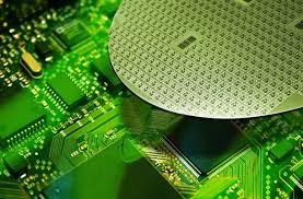
At the heart of all modern electronics lies the semiconductor — a class of materials capable of both conducting and insulating electrical current under different conditions. The cornerstone of this field is the semiconductor silicon wafer, the substrate upon which integrated circuits (ICs) are built. Its atomic precision, crystalline purity, and capacity for controlled modification make it indispensable for computing, communications, and power devices.
From a materials science perspective, silicon’s utility arises from its tetrahedral lattice and bandgap energy of 1.12 eV at room temperature, providing a balance between conductivity and control. This delicate balance allows doping processes to manipulate charge carriers—electrons and holes—with predictable precision.
The production of semiconductor-grade silicon involves extensive purification, crystal alignment, and surface engineering, transforming raw metallurgical silicon into a foundation for nanoscale architectures.
The Physics of Crystal Growth
Crystal growth is the first and perhaps most critical phase of wafer fabrication. It defines the lattice perfection and electrical homogeneity of the entire batch. The process begins with electronic-grade polysilicon, purified to 99.9999999% (9N) through chemical vapor deposition (CVD) of trichlorosilane (SiHCl₃).
The Czochralski (CZ) Method
Most modern wafers originate via the Czochralski process, where a small seed crystal is dipped into molten silicon and slowly withdrawn under precise temperature gradients. This method allows the alignment of atomic planes, minimizing dislocations. A quartz crucible contains the melt, while argon flow maintains an inert atmosphere, preventing oxygen contamination.
The Float-Zone (FZ) Technique
For applications demanding higher purity—like power transistors and radiation detectors—the Float-Zone method is preferred. A radiofrequency (RF) coil melts a narrow region that moves along the polysilicon rod. Impurities segregate into the molten zone, leaving behind ultrapure solid silicon.
Both methods are governed by thermodynamic equilibrium, nucleation kinetics, and defect diffusion models, ensuring the monocrystalline structure is consistent from center to edge. The final ingot typically measures 200–300 mm in diameter, depending on device scale.
Precision Slicing and Surface Planarization
Once grown, the ingot is trimmed and sliced into thin disks using diamond-coated wire saws. These slices, known as wafers, are only 0.5–1 mm thick. Maintaining parallelism and surface smoothness within nanometer tolerances is essential to avoid distortions in subsequent photolithographic steps.
After slicing, wafers undergo lapping to remove saw marks, followed by chemical-mechanical polishing (CMP) that achieves atomic-level flatness. A key metric here is Total Thickness Variation (TTV), which must remain below a few microns across the wafer.
CMP employs colloidal silica and ammonium-based slurries that chemically soften silicon while mechanically abrading it. Surface roughness (Ra) is often reduced to under 0.5 nm, ensuring a mirror finish ideal for nanofabrication.
Controlled Doping: Engineering Electrical Behavior
The intrinsic silicon lattice is a poor conductor; its true potential emerges through doping, the deliberate introduction of impurities. By adding minute concentrations of trivalent (p-type) or pentavalent (n-type) atoms, engineers create regions with desired charge carriers.
In the case of n-type silicon, phosphorus (P) or arsenic (As) contributes free electrons. For p-type, boron (B) introduces holes. Ion implantation or thermal diffusion governs this modification.
- Ion Implantation: Ions are accelerated by an electric field and embedded into silicon at controlled depths (typically 50–200 nm). Subsequent annealing repairs lattice damage and activates dopants.
- Thermal Diffusion: Dopant atoms migrate through silicon in a high-temperature furnace, driven by concentration gradients. Although less precise than implantation, it is useful for forming uniform junctions.
Doping concentrations range from 10¹⁵ to 10²⁰ atoms/cm³, dramatically influencing resistivity and carrier mobility. The result is a material whose properties can be fine-tuned for diodes, transistors, and integrated circuits.
Oxidation and Surface Chemistry
Thermal oxidation forms one of the most important structures in semiconductor processing—the silicon dioxide (SiO₂) layer. This dielectric film acts as a barrier, insulator, and protective coating, serving multiple roles in device isolation and gate oxide formation.
Dry and Wet Oxidation
- Dry oxidation: Uses pure oxygen at 900–1,200°C, yielding thin, high-quality films for gate oxides.
- Wet oxidation: Introduces water vapor, promoting faster growth rates ideal for thick field oxides.
Oxidation kinetics follow the Deal–Grove model, which balances diffusion through the oxide and reaction at the interface. Factors like substrate orientation (e.g., <100> vs. <111>), temperature, and pressure affect oxide growth rates.
The interface between Si and SiO₂ is chemically stable and electrically clean, making it the foundation for the MOS (metal-oxide-semiconductor) structure—the building block of modern electronics.
The Art and Science of Photolithography
Photolithography translates circuit designs into physical patterns on wafers. It is a process combining optics, chemistry, and precision mechanics at nanometer scales.
A layer of photoresist—a light-sensitive polymer—is spin-coated onto the wafer surface. Using ultraviolet (UV) light, patterns are projected through a mask that defines circuit geometries. Exposed regions of the photoresist undergo chemical changes, enabling selective removal during development.
Key Process Steps:
- Coating: Uniform resist film applied at 2,000–5,000 rpm.
- Soft Bake: Solvent removal to stabilize resist properties.
- Exposure: Deep UV (DUV) or extreme UV (EUV) sources define nanoscale features.
- Development: Chemical dissolution of exposed or unexposed regions, depending on resist type (positive or negative).
- Hard Bake: Final curing to enhance adhesion and etch resistance.
Modern lithography achieves resolutions below 10 nm using EUV systems operating at 13.5 nm wavelengths. Alignment precision below 1 nm ensures consistent pattern placement across multiple layers.
Etching and Pattern Definition
After photolithography, etching removes selected material areas to create functional patterns. Two main techniques dominate: wet etching and dry etching.
Wet Etching
Involves chemical dissolution using acids like hydrofluoric (HF) or nitric (HNO₃). Wet methods offer high selectivity but limited anisotropy, meaning features can undercut masked regions.
Dry Etching
Uses plasma or reactive ion environments (RIE). Ions accelerated toward the wafer physically and chemically remove material in a controlled, directional manner. This process allows for sub-10 nm feature definition, vital for modern transistor geometries.
Etching uniformity and selectivity depend on gas composition, chamber pressure, and RF power. Common gases include Cl₂, BCl₃, and SF₆. Engineers monitor endpoint detection through optical emission spectroscopy to ensure layer precision.
Thin Film Deposition and Layer Integration
Deposition processes build up additional layers that form conductive, insulating, or barrier materials. They occur through chemical vapor deposition (CVD), physical vapor deposition (PVD), or atomic layer deposition (ALD)—each offering distinct control over thickness, conformity, and film purity.
- CVD: Reactant gases decompose on the wafer surface, forming solid films like Si₃N₄ or polysilicon. Parameters such as gas flow, temperature, and pressure determine film density and stress.
- PVD: Uses sputtering or evaporation to deposit metals (e.g., Al, Cu, W) essential for interconnects.
- ALD: Alternating gas pulses deposit one atomic layer per cycle, ideal for ultra-thin gate oxides and high-k materials.
Interface quality, stress management, and thermal expansion matching are central to maintaining device integrity. Each film must adhere uniformly while preserving crystalline alignment and electrical isolation.
Testing, Inspection, and Metrology
Before being assembled into devices, wafers undergo extensive testing to detect structural and electrical anomalies.
Physical Inspection
Optical and electron microscopy reveal dislocations, slip lines, and surface particles. Tools like atomic force microscopy (AFM) measure roughness at sub-nanometer scales.
Electrical Characterization
Techniques such as four-point probe measurements, Hall effect analysis, and CV profiling determine resistivity, carrier concentration, and interface quality.
Defect Metrology
Non-destructive methods—like laser scattering and photoluminescence mapping—quantify defect density. The threshold for advanced logic devices often requires fewer than one defect per square centimeter.
Yield improvement relies on statistical process control (SPC), enabling manufacturers to maintain consistent output across thousands of wafers per batch.
Integration of Advanced Semiconductor Wafers
The evolution of semiconductor technology demands increasingly complex wafer architectures. The introduction of strained silicon, silicon-on-insulator (SOI), and compound semiconductors expands design flexibility and performance thresholds.
The term semiconductor wafers encompasses not only pure silicon substrates but also materials like gallium arsenide (GaAs), silicon carbide (SiC), and gallium nitride (GaN). These alternatives support high-power, high-frequency, and radiation-tolerant applications.
For instance, SiC wafers excel in high-voltage switching due to their wide bandgap (3.2 eV) and high thermal conductivity. GaN-based wafers, on the other hand, dominate in RF and optoelectronic fields, leveraging superior electron mobility.
Each material system requires tailored growth techniques, lattice matching considerations, and interface engineering to mitigate dislocation densities and thermal stresses.
Thermal Management and Reliability Science
Thermal stability defines the operational longevity of devices fabricated on semiconductor wafers. The complex interplay between Joule heating, thermal conductivity, and interface diffusion determines how heat dissipates under load.
Silicon’s thermal conductivity (~150 W/m·K) allows efficient heat spreading, but as device geometries shrink, heat flux densities increase exponentially. Engineers mitigate this through backside thinning, metal heat spreaders, and low-k dielectrics to reduce parasitic capacitance.
Reliability testing involves accelerated stress experiments—thermal cycling, high-temperature storage, and electromigration analysis—to predict mean time to failure (MTTF) under real-world conditions.
Nanostructuring and Surface Modification
Modern semiconductor engineering integrates nanostructured surfaces to enhance electrical, optical, and mechanical performance. Techniques like nanoimprint lithography, self-assembled monolayers (SAMs), and plasma texturing introduce nanoscale roughness or patterning that affects charge transport and light reflection.
Atomic layer etching (ALE) and plasma oxidation allow single-atomic-layer control over surface chemistry, facilitating integration with quantum devices, MEMS sensors, and photonic circuits.
The intersection of surface science and quantum physics marks the frontier of next-generation wafer technology, where defect engineering and strain modulation enable entirely new device paradigms.
Conclusion
The fabrication of semiconductor wafers stands as a masterclass in multidisciplinary engineering—bridging chemistry, physics, thermodynamics, and precision manufacturing. Each stage, from crystal growth to nanostructuring, contributes to an ecosystem of atomic-level control that underpins every modern technology.
Understanding these processes at a materials science level not only explains how our digital world functions but also illuminates the challenges of scaling to ever smaller dimensions. As research advances, innovations in wafer materials, processing environments, and metrology will define the next era of electronic performance and reliability.