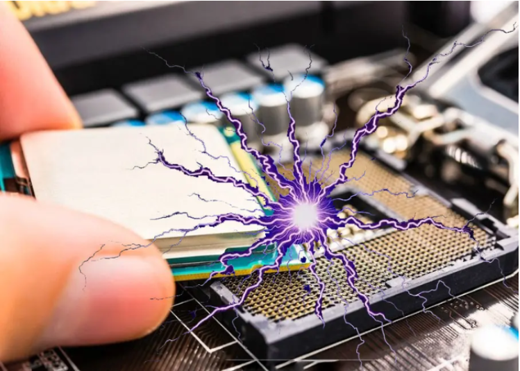
Electrostatic Discharge (ESD) is a sudden flow of electricity between charged objects, posing a significant threat to electronic components. This invisible event can cause immediate or delayed failure, making it a critical concern in manufacturing, handling, and using modern electronics. The damage occurs when the immense energy from a discharge overwhelms a component’s delicate internal structures.
The destructive power of ESD manifests through three primary physical mechanisms: thermal damage, electric field breakdown, and current-induced damage. The instantaneous high current generates intense local heat, which can melt or vaporize microscopic metal interconnects and semiconductor junctions within a chip. Simultaneously, the extremely high voltage creates a powerful electric field that can puncture and destroy thin insulating layers, particularly the vulnerable gate oxide in MOS transistors. Furthermore, the rapid current surge can cause electromigration, physically dislodging metal atoms and leading to open or short circuits.
ESD damage presents in two forms: catastrophic and latent. Catastrophic failure is immediate and obvious, rendering the component completely non-functional. Latent damage is more deceptive; the device appears operational but suffers from degraded performance, such as increased leakage current or parameter drift. This hidden ESD damage significantly shortens the component’s lifespan, leading to premature failure in the field, which is often more costly and difficult to diagnose.
The sensitivity to ESD varies greatly among components. Modern micro-scale devices with finer geometries are exceptionally vulnerable. MOS integrated circuits, precision operational amplifiers, microwave components, and advanced logic families (like HC/HCT) are highly susceptible. LEDs, lasers, and VLSI chips are also notoriously ESD-sensitive due to their fragile internal structures.
Three main models describe how ESD events occur: the Human Body Model (HBM), simulating a discharge from a person; the Charged Device Model (CDM), where the component itself becomes charged and discharges upon contact; and the Field-Induced Model (FIM), where an external electrostatic field induces damaging voltages within the chip.
The failure symptoms depend on the circuit type. In digital circuits, ESD damage often results in increased leakage current or complete functional loss. Linear and analog circuits may exhibit increased offset voltage, noise, or drift in precision resistors. Common physical damage includes burnt metalization, blown protection diodes, and punctured gate oxides.
Preventing this pervasive threat requires a comprehensive strategy. Effective protection begins with circuit design that incorporates dedicated on-chip protection structures like transient voltage suppression (TVS) diodes. During manufacturing and handling, a strict Electrostatic Protected Area (EPA) is essential. This involves using anti-static wrist straps, conductive floor mats, ionizers, and proper shielding packaging materials. Controlling environmental humidity and ensuring all personnel and equipment are properly grounded are also fundamental practices.
In conclusion, ESD causes component failure through the devastating effects of extreme heat, overpowering electric fields, and destructive current surges. The resulting ESD damage can be either immediately catastrophic or insidiously latent. As electronic components continue to shrink, their susceptibility to ESD increases. Therefore, a vigilant and multi-layered approach to ESD prevention—encompassing design, production, and handling protocols—is not just beneficial but absolutely essential for ensuring the reliability and longevity of electronic products.